Schematics for Lunch
The thing I had been avoiding
I have been putting off KiCad for weeks. Not because I didn’t know I needed to learn it. Because I did know, and it looked hard, and I am extremely good at finding reasons to do other things instead.
Today I ran out of other things.
The coworking space plan
I had a four-hour block between meetings in the city. The plan was reasonable: hit the coworking space, knock out a few different things on the list, maybe grab lunch, take a walk. It was genuinely nice weather. I had noted the nice weather specifically. I was going to experience it.
I opened KiCad to “get familiar with the interface a bit more.”
Six hours later
I did not get familiar with the interface. I built a PCB.
I also did not have lunch. I did not take a walk. The weather remained nice without my participation. At some point the coworking space got quieter around me and I did not notice that either.
This is what flow state actually feels like, I think. Not productive and focused. More like: you look up and time has done something strange.
What I was building
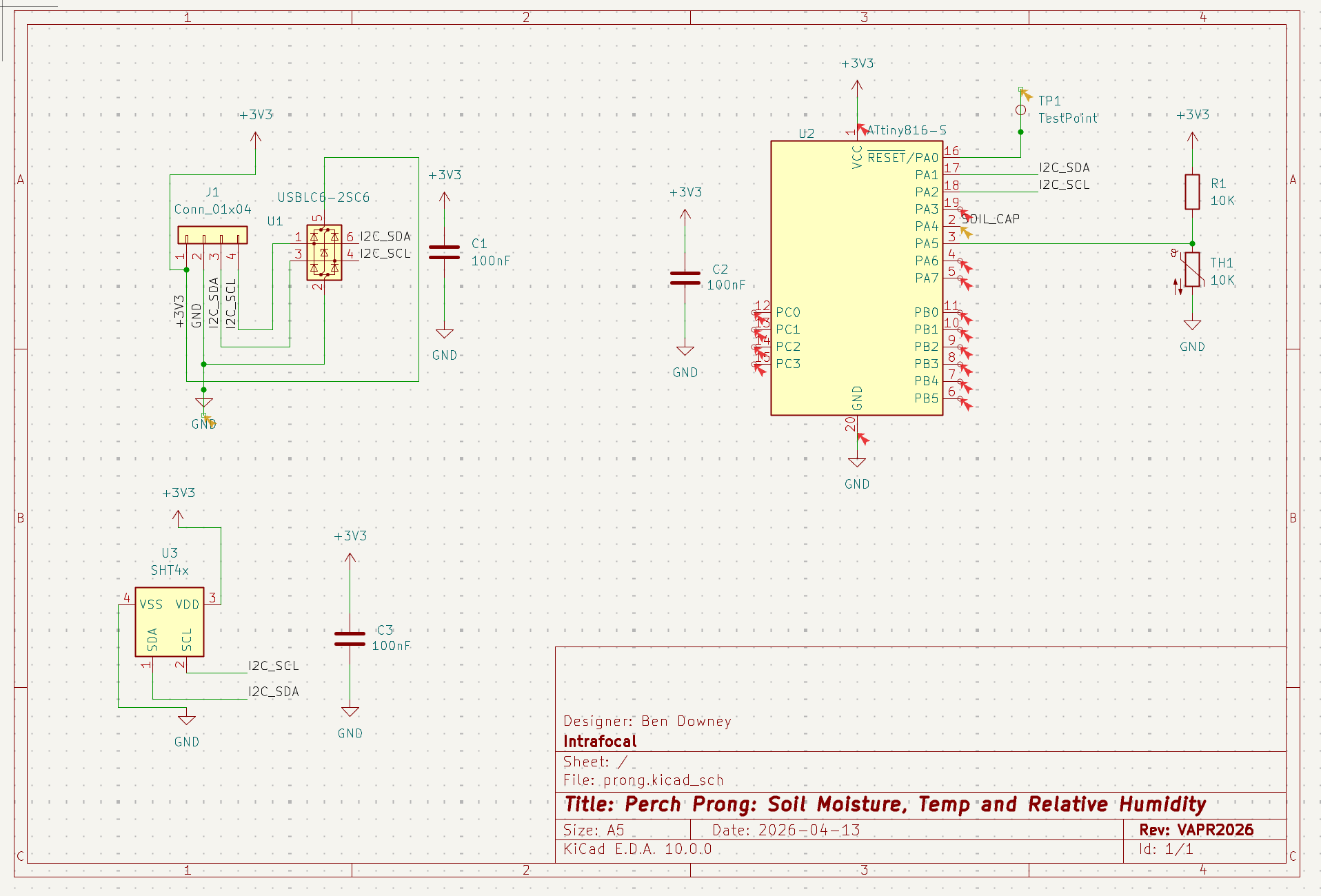
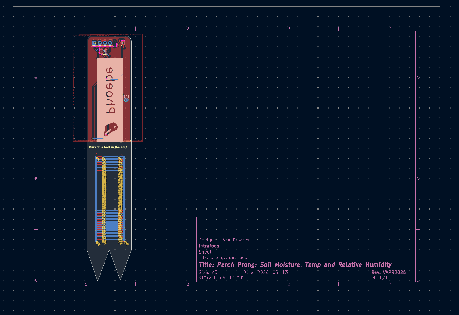
The soil sensor probe. This was supposed to be the easy one. A known design pattern: capacitive soil moisture sensing is a solved problem, there are reference designs everywhere, and I just needed to adapt one for the Phoebe sensor suite. Simple. Introductory, even.
KiCad did not get that memo.
What actually challenged me
Schematic capture was fine. Pleasantly logical. You place components, you draw nets, you label things. My limited electronics knowledge was enough to get through it without too much pain.
Then I opened the PCB editor.
The PCB editor is a different discipline. You’re not thinking about what connects to what anymore. You’re thinking about where things live in physical space, how current actually flows through copper, what happens when two traces run next to each other, why the ground plane looks like that. It’s the difference between a wiring diagram and actual wiring. My brain, which had been coasting on schematic logic, suddenly had to engage a different set of muscles.
Spatial reasoning muscles. My weakest ones, as previously documented.
The part that made it click
Somewhere in hour four I stopped fighting the tool and started thinking like the tool wanted me to think.
The closest analogy I have is TRON. You are a program. You are inside the grid. You are routing light cycles through a digital landscape of sublime geometric logic. Except your hand has cramped into a claw shape, there is a headache building behind your left eye that you are choosing to ignore, and you just routed three traces in the wrong direction because you forgot which layer you were on. Again.
But spiritually: TRON.
Traces are not wires you draw. They’re paths current will actually take, and current has preferences. Ground pours aren’t just a shortcut for wiring GND everywhere. They’re a return path, and where you place your vias matters. The probe tines need to be thermally isolated from the rest of the board or the temperature sensor reads the PCB instead of the soil.
That last one took me an embarrassingly long time to figure out. Thin traces between the tines and the rest of the board. Not a width mistake. A feature.
The renders
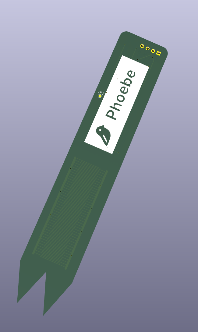
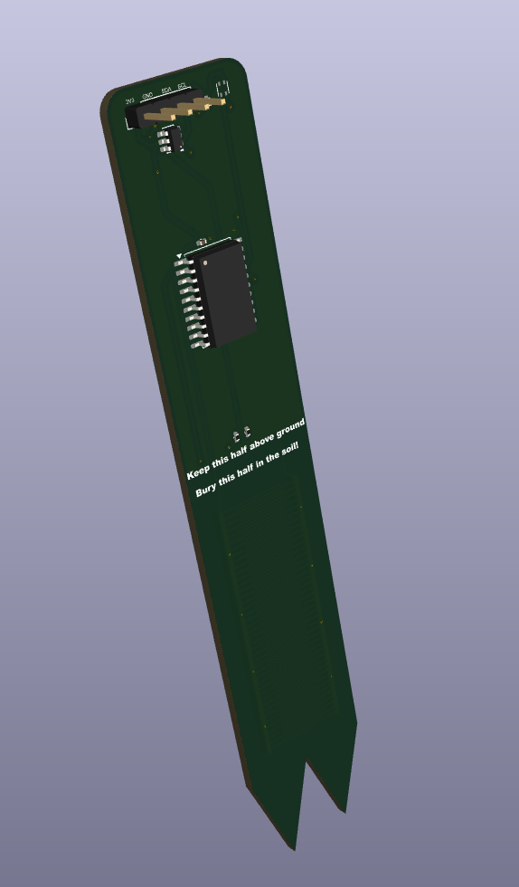
KiCad has a 3D renderer and it is genuinely delightful. You spend six hours staring at a flat copper diagram and then you hit a button and it shows you the actual object. The thing that will (maybe) arrive in a padded envelope from JLCPCB in two weeks.
It might even work.
Questionable but submitted
The honest answer is I don’t know if this board is correct. I know the schematic captures the right circuit. I know the layout passes the DRC. I know the ground plane is poured and the traces are the right width and the thermal isolation is intentional.
Whether it actually works is a question for the assembled board and a bag of soil.
What I do know is that I sat down intimidated by a piece of software and stood up six hours later with a design file. Skipped lunch, skipped the park, skipped any pretense of being a person who takes breaks. And I’d do it again tomorrow.
There is something genuinely intoxicating about the moment theory becomes a physical object. About routing a trace and understanding, for the first time, why it goes where it goes. About a concept you read about becoming a decision you make.
Who needs sunshine and sustenance when you can think about thermal isolation and net integrity.
— Ben